


Transistors this small are approaching the size of individual atoms. IBM packed 100 billion of them onto a fingernail-sized chip using a new three-dimensional architecture called nanostack. The result: 50% more performance or 70% better energy efficiency versus IBM’s 2 nm chips. Commercial production is five years away. The physics just got extended by a decade.
IBM shared a 0.7 nm nanostack chip breakthrough from IBM Research in Yorktown Heights, New York — and the claim it makes is historic. IBM unveiled a major semiconductor breakthrough with the introduction of the world’s first sub-1 nanometre chip technology, featuring a revolutionary transistor architecture at the 0.7 nm, or 7 angstrom, node.
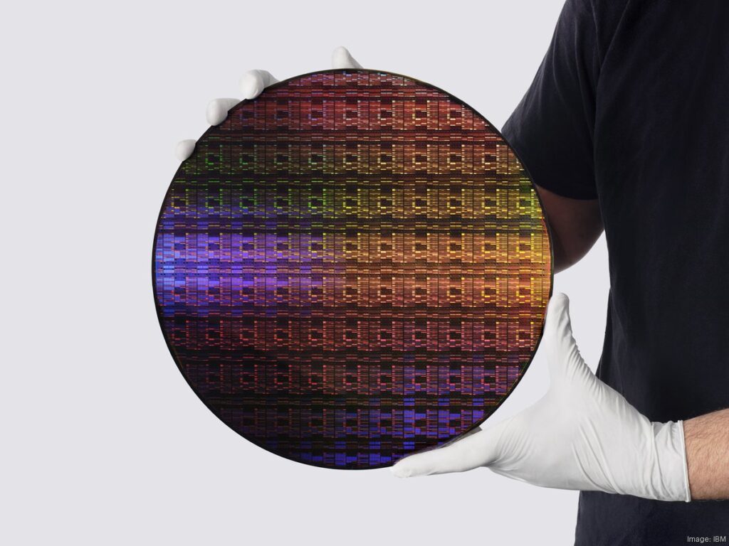
A nanometre is one-billionth of a metre. An angstrom is one-tenth of a nanometre — and the width of a single hydrogen atom. IBM’s new sub-1 nm chip packs nearly 100 billion transistors onto a chip the size of a fingernail, nearly twice the density of IBM’s 2 nm chip unveiled in 2021.
The performance projection is equally striking. Published technical results project the new chip to offer up to 50% more performance, or 70% greater energy efficiency than IBM’s 2 nm node chips — supercharging compute for applications ranging from generative AI and cloud infrastructure to next-generation electronic devices.
Commercial production is not coming tomorrow. IBM projects the earliest adoption within the next five years. By contrast, the physics just demonstrated something that many researchers believed would require entirely new materials to achieve.
What’s Happening & Why It Matters
What 0.7 nm Means
IBM’s 0.7 nm nanostack chip breakthrough requires a specific and honest clarification. The company said the 0.7 nm label refers to a generation of manufacturing technology rather than the exact physical size of every transistor feature. At such advanced nodes, dimensions are increasingly described in angstroms, with one angstrom equal to one-tenth of a nanometre. The semiconductor industry has used this naming convention for years — Intel and TSMC’s “7 nm” and “5 nm” chips, for example, describe process generations rather than literal dimensions. By contrast, IBM‘s 0.7 nm is genuinely different from prior naming conventions in one important way. At this scale, the features being built approach the diameter of individual silicon atoms. The name is no longer purely conventional. It is approaching a physical description.
IBM validated this technology through working hardware — not just simulation. IBM said it had validated the architecture through working transistor structures and a functional CMOS inverter, a basic building block used in digital chips. A functional CMOS inverter is the most fundamental digital logic structure — and demonstrating it at 0.7 nm means the transistors are not just theoretically possible, they switch correctly under test conditions.
The Nanostack Architecture — Stacking Transistors in Three Dimensions
IBM’s 0.7 nm nanostack chip breakthrough rests on a specific architectural innovation. IBM’s nanostack architecture vertically stacks and staggers transistors, allowing more components to be packed onto a chip while enabling different materials to be optimised independently for performance and power efficiency.
Traditional transistors are flat on the surface of a chip — a two-dimensional arrangement that has driven Moore’s Law for six decades by making each transistor smaller and placing more of them side by side. Additionally, that two-dimensional approach is approaching a hard physical limit. Transistors cannot be made indefinitely smaller while remaining flat — quantum tunnelling effects cause current leakage at dimensions below approximately 2 nm. Nanostack responds to that limit by adding a vertical dimension. Instead of spreading transistors across a flat surface, IBM stacks them in three-dimensional columns — allowing more components per unit of surface area without requiring each individual transistor to be any smaller in its critical dimension. Different materials can be used in different layers of the stack — optimising each layer independently for speed or power consumption. That flexibility is the key advantage nanostack provides over earlier three-dimensional architectures like Intel’s FinFET.
The SRAM Breakthrough — for AI
IBM’s 0.7 nm nanostack chip breakthrough delivered a second result alongside the transistor density announcement. IBM researchers demonstrated that the nanostack architecture provides 40% scaling in SRAM, unlocking the ability of chip designers to create much more efficient chips while supporting the high-bandwidth data demands of advanced AI workloads. More compact SRAM could help feed data faster to artificial intelligence chips, where memory bandwidth is a major bottleneck.
SRAM — Static Random-Access Memory — is the fast-access memory placed closest to the processor. Every time a chip performs a calculation, it draws the data it needs from SRAM. As AI models grow larger, they require faster and more capacious SRAM to avoid the processor waiting for data to arrive from slower memory tiers. The AI chip performance limitation most researchers currently flag is not compute speed — it is memory bandwidth. A 40% improvement in SRAM scaling from nanostack addresses precisely that bottleneck. Additionally, IBM presented the SRAM results at VLSI 2026 — the Symposia on VLSI Technology and Circuits — one of the semiconductor industry’s most prestigious annual peer review venues. The results are not a press release claim. They are peer-reviewed research.
The Albany Research Facility Partnership
IBM’s 0.7 nm nanostack chip breakthrough did not emerge from a single laboratory. IBM and its partners conduct the work at a leading semiconductor research facility in Albany, New York, which will soon be home to a High Numerical Aperture Extreme Ultraviolet (High NA EUV) lithography tool, essential for the future of logic scaling. Developed by ASML, the technology enables ultra-precise circuit printing, supporting the creation of smaller, more powerful chips.
IBM’s partners include Lam Research Corp., Tokyo Electron (TEL), and SCREEN Semiconductor Solutions. Lam Research provides the etch and deposition equipment that creates transistor structures. Tokyo Electron provides semiconductor production equipment. SCREEN Semiconductor Solutions provides wafer cleaning equipment. Together, they represent the core toolchain required to actually manufacture chips at the dimensions. By contrast, the High NA EUV tool from ASML — the Dutch lithography manufacturer that holds a virtual monopoly on the extreme ultraviolet machines required for advanced chip manufacturing — is the most critical piece of infrastructure still pending at Albany. Once that tool arrives and is operational, the facility will have every component needed to manufacture chips at sub-1 nm scale.
In the Global Chip Race
IBM’s 0.7 nm nanostack chip breakthrough arrives directly alongside the two most significant concurrent semiconductor stories of 2026. As TF covered in its China supercomputer article, China’s LineShine supercomputer topped the global TOP500 ranking using CPU-based architecture — built specifically because US export controls denied China access to advanced GPUs. And as TF covered in its Apple price increases article, AI data centres have quadrupled memory chip costs, generating the supply crisis causing Apple to raise iPhone prices.

TSMC — which manufactures chips for Apple, NVIDIA, and AMD — is targeting 2 nm for 2025 volume production and is developing its own 1.4 nm and 1 nm roadmap. Samsung has similar plans. IBM‘s 0.7 nm announcement places the company’s research capability ahead of both TSMC and Samsung’s current published roadmaps — but IBM is a research organisation, not a volume chip manufacturer. IBM will license the technology to manufacturers and partners rather than producing chips at commercial scale itself.
The Physical Limits — and What Nanostack Extends
The semiconductor industry has discussed the “end of Moore’s Law” for more than a decade. Moore’s Law — the observation that transistor density doubles approximately every two years — held from 1965 through approximately 2020. Beyond that point, physical limits, manufacturing complexity, and cost have all constrained the pace of improvement. IBM Research director Jay Gambetta addressed this. “IBM’s latest chip breakthrough is a landmark moment in computing, driving technology beyond the nanometre era to the scale of atoms.”
Nanostack does not defeat physics. By contrast, it navigates the physical limits of two-dimensional scaling by adding a third dimension — an approach that extends the runway for density improvements without requiring transistors to become individually smaller. At 0.7 nm, transistor features are approaching the size of silicon atoms themselves — approximately 0.2 nm in atomic radius. Whether nanostack can extend below 0.7 nm is an open research question. For now, it has demonstrated that the limits researchers assumed were imminent can be pushed beyond the 2D roadmap suggested.
TF Summary: What’s Next
IBM projects the earliest commercial adoption of 0.7 nm nanostack technology within five years — placing the first commercial chips at thie node in approximately 2031. The Albany ASML High NA EUV installation provides the manufacturing foundation when operational. IBM will publish full technical details of the VLSI 2026 presentation. Partners Lam Research, Tokyo Electron, and SCREEN continue development work at Albany.
MY FORECAST: IBM’s 0.7 nm nanostack chip breakthrough will accelerate TSMC and Samsung‘s sub-1 nm roadmaps by demonstrating the nanostack architecture is physically viable and not merely theoretical. Both foundries will announce their own nanostack-adjacent programmes within 18 months — they cannot allow a research organisation to own the public narrative on the next node without responding. By contrast, the commercial timeline matters more than the research announcement. Five years to first commercial adoption is a long runway in a semiconductor cycle that is simultaneously being compressed by AI demand, US-China competition, and hyperscaler capex. The first production chips at or near 0.7 nm will likely arrive from TSMC or a successor node before 2031 — because the AI spending cycle is creating the demand pressure that makes faster commercialisation economically necessary. IBM found the path. The volume manufacturers will determine when the world actually walks it.
Related Stories
- China Tops Global Supercomputer Rankings and Opens the World’s First Underwater Data Centre
- OpenAI and Broadcom Unveil Jalapeño — a Custom AI Chip Built to Cut NVIDIA Costs by 50%
- Tim Cook Confirms Apple Price Rises — Memory Crunch and Intel’s US Chips Are Why