



$6.3 billion. One shared factory. TSMC’s manufacturing muscle, Sony’s sensor expertise, and a bet that the next big camera customer isn’t a phone at all. It’s a robot.
Sony and TSMC are planning to spend around $6.3 billion on a joint venture to produce advanced image sensors in Japan, according to Nikkei and confirmed by multiple sources familiar with the talks. The venture will be 60% owned by Sony, 40% by TSMC, with commercial production targeted as early as 2029 at Sony’s existing sensor campus in Kumamoto Prefecture. Neither company has confirmed the figure officially. Sony declined to comment. TSMC didn’t respond to requests for comment.
What’s Happening & Why It Matters
Fab-Light, One Step at a Time
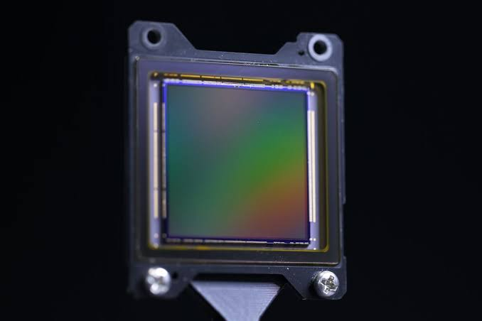
This isn’t Sony’s first pivot away from doing everything in-house. Sony’s chief executive, Hiroki Totoki, called the arrangement the company’s “first step to becoming fab-light” when the two companies signed their preliminary agreement back in May. Sony handled sensor research, design, and manufacturing, start to finish. TSMC brings the manufacturing scale and process technology; Sony brings decades of sensor design expertise that made it the world’s largest maker of image sensors in the first place.
Analyst Hideki Yasuda at Toyo Research Advice said: “This is a virtually risk-free investment for Sony and TSMC.” The arrangement eases Sony’s capital burden in a business where massive manufacturing spend is unavoidable, while giving TSMC a reliable revenue stream outside its core logic-chip business.
The Real Customer Isn’t a Phone
Sony still supplies premium sensors to Apple, Huawei, and Samsung — and the venture will keep those iPhone camera contracts running. But the companies are explicit that the longer game is elsewhere. Both firms said the partnership will explore “physical AI” applications: autonomous vehicles, industrial robots, AI-driven object recognition. Cars and robots need to see the world, in real time, and that’s a sensor problem before it’s ever a software problem.:
TSMC gets something specific out of that shift too. The company wants expertise in physical AI, and partnering with the world’s dominant sensor maker is a faster path there than building that knowledge alone.
$6.3 Billion Against a Bigger Backdrop
There is important context. The investment is four years’ worth of Sony’s semiconductor capital spending in a single project, and it is close to the $8.6 billion TSMC already sank into its first Kumamoto logic-chip fab. Sony still faces real competition — Samsung and China’s OmniVision are both chasing its lead in image sensors, even as Sony controls more than half the global CMOS sensor market today.
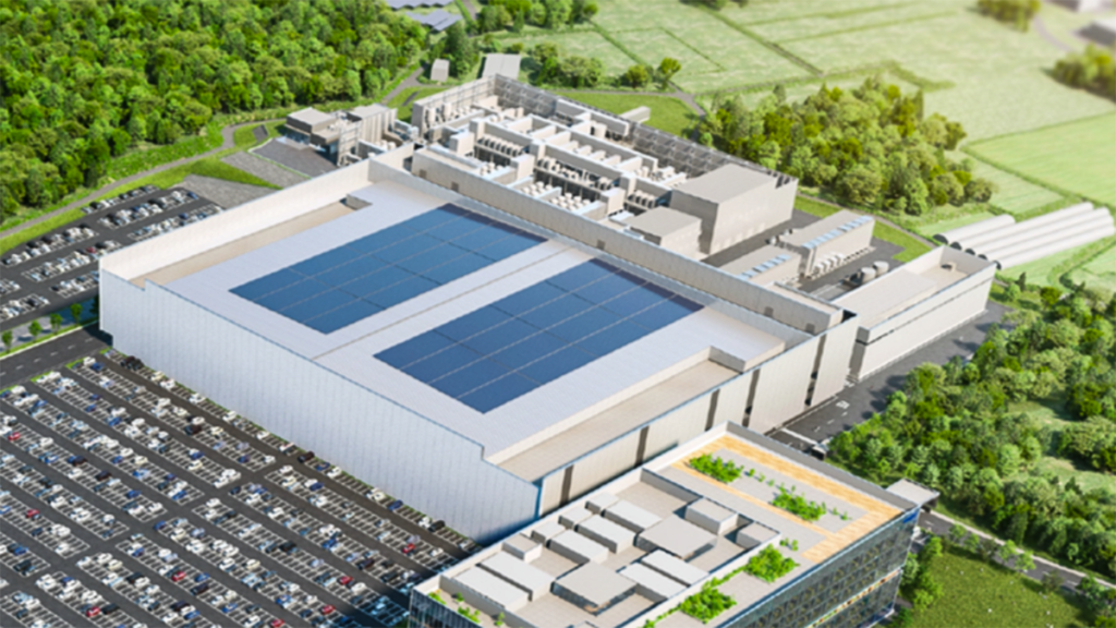
Sony isn’t handing over everything, either. The company is expected to keep its most proprietary manufacturing processes to itself, even as TSMC takes a meaningful stake in the new venture. Japan’s government is watching, too. Trade Minister Ryosei Akazawa said Tokyo will consider financial support for the project, a signal of how central chip sovereignty is to Japanese industrial policy.
TF Summary: What’s Next
The joint venture is expected to be established by the end of Sony’s fiscal year 2026, which runs through March 2027. Commercial production targets 2029 at the Kumamoto facility. No confirmed timeline exists yet for when the investment itself gets deployed. Japanese government financial support is under consideration, not yet finalised.
MY FORECAST: Expect the venture to be the template for how established consumer-electronics chipmakers handle the capital intensity of next-generation manufacturing — partner with a foundry giant rather than build alone, and keep the design IP in-house while outsourcing the expensive part. Watch for Samsung to respond with a comparable sensor-manufacturing partnership of its own within the next year, given how the deal targets Samsung’s own position in the same market. The physical AI angle is the one to track longer term. If autonomous vehicles and industrial robotics scale the way both companies are betting, image sensors stop being a smartphone component and start being foundational infrastructure — and whoever locks in that supply chain first gets a multi-year head start.
Related Stories
- Chinese Memory Chipmaker CXMT Surges on Stock Market Debut
- IBM Claims the World’s First Sub-1-Nanometre Chip Technology
- Micron Breaks Ground on a $9.3 Billion Chip Plant in Japan